Single-layer vs. Double-layer PCBs: What’s the Difference?
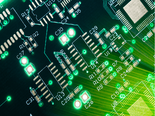
Printed circuit boards (PCBs) are an integral part of modern electronics, providing a platform for mounting and connecting electronic components using conductive tracks, pads, and features. There are different types of PCBs available, and in this post, we will focus on single-layer and double-layer PCBs.
Single-layer PCBs
A single-layer PCB, as the name suggests, is a PCB with only one layer of conductive material. These PCBs are made by etching a pattern of conductive tracks onto a single layer of a substrate material, usually a thin sheet of fiberglass or composite material. The etching process involves applying a thin layer of copper onto the substrate and then using a photolithographic process to remove unwanted copper and leave behind the desired pattern. The remaining copper is then coated with a layer of protective insulation called the solder mask, which helps to prevent accidental short circuits and makes the PCB more durable.
There are several advantages to using single-layer PCBs. One of the main advantages is cost: single-layer PCBs are generally less expensive to manufacture than double-layer PCBs due to their simplicity. Single-layer PCBs are also easier to manufacture and require less specialized equipment, making them a good choice for small-scale projects or prototypes.
However, there are some limitations to using single-layer PCBs. One of the main limitations is space: with only one layer available, there is limited space for components, which can be a problem for more complex circuits. Single-layer PCBs also tend to have less reliable signals, as the conductive tracks are more susceptible to interference and crosstalk. Additionally, single-layer PCBs are less durable than double-layer PCBs, as they are more prone to damage from bending or impact.
Double-layer PCBs
A double-layer PCB, on the other hand, is a PCB with two layers of conductive material separated by a substrate material. These PCBs are made by bonding two single-layer PCBs together, with the conductive tracks on one layer facing the conductive tracks on the other layer. The bonding process involves applying a layer of adhesive and then pressing the two layers together under high pressure. The result is a PCB with two layers of conductive tracks that are electrically isolated from each other by the substrate material.
Double-layer PCBs offer several advantages over single-layer PCBs. One of the main advantages is space: with two layers available, there is more space for components, which is useful for more complex circuits. Double-layer PCBs also have better signal integrity, as the conductive tracks are less susceptible to interference and crosstalk due to the isolation provided by the substrate material. Additionally, double-layer PCBs are more durable than single-layer PCBs, as they are less prone to damage from bending or impact.
However, there are some limitations to using double-layer PCBs. One of the main limitations is cost: double-layer PCBs are generally more expensive to manufacture than single-layer PCBs due to their complexity. Double-layer PCBs also require more specialized equipment and a more complex manufacturing process, which can be a barrier for small-scale projects or prototypes.
Comparison of Single-layer and Double-layer PCBs
When deciding between single-layer and double-layer PCBs, it is important to consider the trade-offs in terms of cost, complexity, space for components, signal integrity, and durability. Single-layer PCBs are generally less expensive and simpler to manufacture, but they have limited space for components and may not be suitable for more complex circuits. Double-layer PCBs, on the other hand, offer more space for components and better signal integrity, but they are more expensive and require a more complex manufacturing process.
In general, single-layer PCBs are a good choice for simple circuits that do not require a lot of components or for prototypes and small-scale projects where cost is a major concern. Double-layer PCBs are a better choice for more complex circuits that require a lot of components or for applications where signal integrity and durability are important.
It’s also worth noting that there are other types of PCBs available beyond single-layer and double-layer, such as multi-layer PCBs (which have three or more layers) and flex PCBs (which are made of flexible materials). These types of PCBs offer even more space and flexibility, but they are generally even more expensive and complex to manufacture.
Conclusion
In conclusion, single-layer and double-layer PCBs are two different types of PCBs that offer different trade-offs in terms of cost, complexity, space for components, signal integrity, and durability. Single-layer PCBs are a good choice for simple circuits and prototypes, while double-layer PCBs are a better choice for more complex circuits and applications that require better signal integrity and durability. When choosing between single-layer and double-layer PCBs, it is important to consider the specific needs of your project and weigh the pros and cons of each type.